�߾��ȣ��ͳɱ�����Դʹ��AD8276��ַŴ�����AD8603����Ŵ��� Circuit Function and Benefits
Current sources are widely used in industrial, communication, and other equipment for sensor excitation and machine-to-machine communication, etc. For example, the 4 mA-to-20 mA loop is widely used in process control equipment.
Programmable current sources can be built using a DAC, amplifier (op amp or difference amplifier), and matched resistors. Low value current sources can be integrated into low output current sources or amplifiers. For example, the AD8290 is an instrumentation amplifier with a single integrated current source, and the AD7794 is a high resolution ��-�� ADC with two integrated current sources. For high currents, external MOSFETs or transistors will generally be required.
Current sources using the low power AD8276 difference amplifier and the AD8603 op amp are affordable, flexible, and small in size. Performance characteristics such as initial error, temperature drift, and power dissipation are excellent.
<-- popup for enlarge -->High Precision, Low Cost Current Sources Using the AD8276 Difference Amplifier and the AD8603 Op Amp (CN0099)

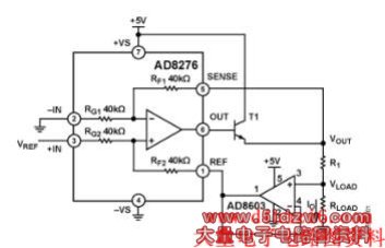
Figure 1: Current Source Using the AD8276 Difference Amplifier and the AD8603 Op Amp (Simplified Schematic)
|
| Figure 1: Current Source Using the AD8276 Difference Amplifier and the AD8603 Op Amp (Simplified Schematic) |
The current source circuit is shown in Figure 1. Reference voltage, VREF, is applied to the noninverting input of the AD8276. This voltage controls the amount of output current, IO. The inverting input of the AD8276 is connected directly to ground. There are four laser-trimmed, 40 k�� resistors inside the AD8276 that are connected to the input pins, the REF pin, and the SENSE pin. The output of the AD8276 is used to drive a transistor if a high current output is needed.
If the resistors are perfectly matched, the input voltage, VREF, appears across R1, thereby producing a constant load current, IO, which is equal to VREF/R1.
The AD8603 op amp is used in the feedback loop of the circuit and was chosen because of its low bias current (maximum 1 pA) and offset voltage (less than 50 ��V). The low bias current makes it possible to interface to a high impedance load without introducing significant offset errors. The AD8603 low temperature drift specification (4.5 ��V/��C maximum) allows operation over a wide temperature range, and the amplifier also features low noise and rail-to-rail inputs and outputs.
The value of the output current, IO, can be calculated by using the equation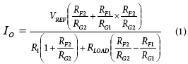
Because the AD8276 has very tight resistor matching, RF1/RG1 = RF2/RG2 = 1, and Equation 1 can be simplified as ![]()
Equation 1 shows that the primary errors of the circuit in Figure 1 are due to the internal resistor matching, the tolerance of R1, and the tolerance of the load resistance. The AD8276 (B-grade) maximum gain error is 0.02%. The AD8276 (A-grade) maximum gain error is 0.05%. Overall accuracy of 0.02% is possible with the circuit.
At the same time, the accuracy of R1 is critical, so it should have 0.1% tolerance or better. This error can be removed by calibration.
The amount of output current, IO, available from the circuit is limited by the op amp input range, the difference amplifier output range, and the difference amp SENSE pin voltage range.
Based on Figure 1, three conditions have to be met:
- VLOAD = IO �� RLOAD must be within the AD8603 op amp input range.
- VOUT = IO �� (RLOAD + R1) must be within the AD8276 SENSE pin voltage range: 2(−Vs) − 0.2 V to 2(+Vs) − 3 V.
- IO �� (RLOAD + R1) + 2(−Vs) − 0.2 V to 2(+Vs) − 3 V must be within the AD8276 output voltage range: �CVs + 0.2 V to +Vs − 0.2 V.
The AD8276B offset voltage drift of 2 ��V/��C maximum and gain drift of 1 ppm/��C maximum yield low temperature drift and wide temperature operation. The specifications for the AD8276A are 5 ��V/��C and 5 ppm/��C, respectively.
Both the AD8276 (8-lead MSOP) and the AD8603 (5-lead TSOT-23) are in small packages, thereby minimizing the board area required by the circuit.
The external current source transistor, T1, should have a VCB breakdown voltage higher than the AD8276 supply voltage. The transistor maximum collector current should be higher than the expected output current with suitable headroom, and the transistor power dissipation limits must be observed. Low cost transistors, such as the 2N3904, 2N4401, 2N3391, and MPSA06 are recommended.
The AD8276 can drive output currents of 15 mA or less without the need for the external transistor or MOSFET.
Testing results under room temperature based on theAD8276A, AD8603, and 2N3904 are shown in Figure 2. R1 is 50 �� with 0.1% tolerance. It is obvious that the actual output complies with the calculated results. On the scale shown, the measured results are indistinguishable from the ideal results because they are within 0.5% of each other with the average of less than 0.1% limited by the R1's tolerance.
���߾��ȣ��ͳɱ�����Դʹ��AD8276��ַŴ�����AD8603