标签:电路图讲解,电路图练习,http://www.5idzw.com
SST89C58电子盘电路及代码,http://www.5idzw.com
SST89C58 74HC573
Reference design for SST ATA-Disk Chip into 8051 microcontroller
Application note
Abstract: this application note introduces the hardware and firmware of reference design for SST ATA-Disk Chip SST58SD/LDxxx into SST FlashFlex51 SST89C54/58 (8051 compatible microcontroller).
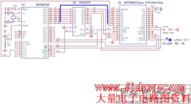
1. Hardware connections:
Please reference to attached schematic diagram for hardware connections.
SST ATA-Disk Chip (ADC) SST58SD/LDxxx only supports one working mode, ie. ATA/IDE mode, all control signals are connected based on Table 2-8, Page 14 on datasheet. After executed Set Feature Command to enable 8-bit data transfers, all higher 8 bit data bus ( D8-D15) are don’t care and can be No Connect. RESET# (pin1) is optional, it can be tied up to Vcc if not used. After power-up, ADC will automatically be reset internally, it doesn’t need external reset input. But it’s a good practice to connect RESET# to one of I/O pins such as P1.4, in case ADC is out of control for any unknown reasons, host MCU has capability to reset ADC. DASP# is connected to an emitting diode through a resistor to Vcc, LED provides user a visibility of ADC’s internal operation. When ADC is active busy on operation, LED will be on. Please be noted that master/slave Selection at CSEL pin won’t take effect until Next reset, in other words, if you change the jumper setting of master/slave selection, you MUST reset ADC once.
If your application system expands any other I/O or data memory, please modify the reference design: (1)change CS3FX# to Vcc, (2)connect the output of address decoder to CS1FX#. When both CS1FX# and CS3FX# are high, ADC is de-selected and be standby state, all data bus are in high-z. When CS1FX# is low, ADC is selected and be operational. So CS1FX# acts as Chip Select (/CS) in most common peripherals.
2. Firmware design guide:
It’s important to know that ATA/IDE standard doesn’t permit access only one byte at a time to its media such as HDD or ADC, firmware must read or write data sector by sector, 1 sector has 512 bytes of data, system design engineer must design data buffer to support random access to ADC. Reference design uses the secondary block (4Kbytes x 8bit) of on-chip flash in SST89C54/58 as data buffer.
After power-up or external reset, ADC is default to be 16-bit operation. As SST89C54/58 is 8-bit MCU, firmware must enable 8-bit operation by Set Features Command, please reference to page 32 on datasheet.
If ADC is set as Slave, other than Master, you need to change the bit4 in Drive/Head Register to be 1 when writing Command to ADC, see page 17 on datasheet.
After power-on or reset, ADC will be ready to read / write operation after 200ms (typical), 500ms (maximum), see page 1 under Start Up Time in Features on datasheet.
3. Conclusion:
It’s easy to modify this reference design to any other embedded controllers as long as you follow above design guidelines.
4. Schematic diagram:
5. 8051 Source code:
; all commands supported by ADC.
ChkPwr Equ 0E5h ; 98h
Diagnostic Equ 90h
Format Equ 50h
Identify Equ 0ECh
Idle Equ 0E3h ; 97h
IdleImm Equ 0E1h ; 95h
Initialize Equ 91h
ReadBuf Equ 0E4h
ReadLong Equ 22h ; 23h
ReadMulti Equ 0C4h
ReadSctr Equ 20h ; 21h
ReadVerify Equ 40h ; 41h
Recalibrate Equ 10h ; 1xh
Seek Equ 70h ; 7xh
SetFeature Equ 0EFh
SetMulti Equ 0C6h
Sleep Equ 0E6h ; 99h
Standby Equ 0E2h ; 96h
StandbyImm Equ 0E0h ; 94h
WriteBuf Equ 0E8h
WriteLong Equ 32h ; 33h
WriteMulti Equ 0C5h
WriteSctr Equ 30h ; 31h
WriteVerify Equ 3Ch
;=============================================================
; ADC Drive Register Set definitions
Data_Reg Equ 8000h ; Data Register for read / write
Error_Reg Equ 8001h ; Error Register, read only
Features Equ 8001h ; features Register, write only
,SST89C58电子盘电路及代码
相关元件PDF下载:
SST89C58 74HC573
Reference design for SST ATA-Disk Chip into 8051 microcontroller
Application note
Abstract: this application note introduces the hardware and firmware of reference design for SST ATA-Disk Chip SST58SD/LDxxx into SST FlashFlex51 SST89C54/58 (8051 compatible microcontroller).
1. Hardware connections:
Please reference to attached schematic diagram for hardware connections.
SST ATA-Disk Chip (ADC) SST58SD/LDxxx only supports one working mode, ie. ATA/IDE mode, all control signals are connected based on Table 2-8, Page 14 on datasheet. After executed Set Feature Command to enable 8-bit data transfers, all higher 8 bit data bus ( D8-D15) are don’t care and can be No Connect. RESET# (pin1) is optional, it can be tied up to Vcc if not used. After power-up, ADC will automatically be reset internally, it doesn’t need external reset input. But it’s a good practice to connect RESET# to one of I/O pins such as P1.4, in case ADC is out of control for any unknown reasons, host MCU has capability to reset ADC. DASP# is connected to an emitting diode through a resistor to Vcc, LED provides user a visibility of ADC’s internal operation. When ADC is active busy on operation, LED will be on. Please be noted that master/slave Selection at CSEL pin won’t take effect until Next reset, in other words, if you change the jumper setting of master/slave selection, you MUST reset ADC once.
If your application system expands any other I/O or data memory, please modify the reference design: (1)change CS3FX# to Vcc, (2)connect the output of address decoder to CS1FX#. When both CS1FX# and CS3FX# are high, ADC is de-selected and be standby state, all data bus are in high-z. When CS1FX# is low, ADC is selected and be operational. So CS1FX# acts as Chip Select (/CS) in most common peripherals.
2. Firmware design guide:
It’s important to know that ATA/IDE standard doesn’t permit access only one byte at a time to its media such as HDD or ADC, firmware must read or write data sector by sector, 1 sector has 512 bytes of data, system design engineer must design data buffer to support random access to ADC. Reference design uses the secondary block (4Kbytes x 8bit) of on-chip flash in SST89C54/58 as data buffer.
After power-up or external reset, ADC is default to be 16-bit operation. As SST89C54/58 is 8-bit MCU, firmware must enable 8-bit operation by Set Features Command, please reference to page 32 on datasheet.
If ADC is set as Slave, other than Master, you need to change the bit4 in Drive/Head Register to be 1 when writing Command to ADC, see page 17 on datasheet.
After power-on or reset, ADC will be ready to read / write operation after 200ms (typical), 500ms (maximum), see page 1 under Start Up Time in Features on datasheet.
3. Conclusion:
It’s easy to modify this reference design to any other embedded controllers as long as you follow above design guidelines.
4. Schematic diagram:
5. 8051 Source code:
; all commands supported by ADC.
ChkPwr Equ 0E5h ; 98h
Diagnostic Equ 90h
Format Equ 50h
Identify Equ 0ECh
Idle Equ 0E3h ; 97h
IdleImm Equ 0E1h ; 95h
Initialize Equ 91h
ReadBuf Equ 0E4h
ReadLong Equ 22h ; 23h
ReadMulti Equ 0C4h
ReadSctr Equ 20h ; 21h
ReadVerify Equ 40h ; 41h
Recalibrate Equ 10h ; 1xh
Seek Equ 70h ; 7xh
SetFeature Equ 0EFh
SetMulti Equ 0C6h
Sleep Equ 0E6h ; 99h
Standby Equ 0E2h ; 96h
StandbyImm Equ 0E0h ; 94h
WriteBuf Equ 0E8h
WriteLong Equ 32h ; 33h
WriteMulti Equ 0C5h
WriteSctr Equ 30h ; 31h
WriteVerify Equ 3Ch
;=============================================================
; ADC Drive Register Set definitions
Data_Reg Equ 8000h ; Data Register for read / write
Error_Reg Equ 8001h ; Error Register, read only
Features Equ 8001h ; features Register, write only
,SST89C58电子盘电路及代码
上一篇:LMl872 基本测试电路图